
I was recently reminded about a very nifty little programmable logic chip that hasn’t seen nearly enough attention from hobbyists and makers. Let me tell you about it.
Working on the Tsunami Kickstarter recently, a backer asked about including a frequency divider on the front end, to allow for higher speed and better accuracy frequency counting. Using a programmable divider in front of the timer capture pin would mean lower software overhead when doing frequency counting, and permit greater accuracy for counting high frequencies: counting 256 iterations of a 2MHz signal gives you more accuracy than counting just one.
My initial reaction was to say that it wasn’t practical to add that functionality at this point in the design, but it set me thinking, and against my better judgement I started to look at the options.
A programmable frequency divider seemed the obvious solution, but the only one that came up on a quick search was obsolete and likely in too large a package. Doing this with separate components would require two ICs - a counter and a demux. Besides, this was all theoretical, right? It’s too late to make significant changes.
Not so long ago, something like this would have been solved using something such as a PAL. Of course, those have since been obsoleted by CPLDs and FPGAs, but even the smallest and cheapest of those have a great many pins and would add significantly to the Bill of Materials cost for my project.
At that point I was reminded of a development kit I bought 6 months ago and hadn’t used, for a neat little series of chips called greenpak3. Greenpaks are something like a modern take on PALs. Each one contains a collection of digital building blocks, such as lookup tables, flipflops, and counters, and a flexible routing matrix that allows you to connect them up as needed. Better yet, they’re cheap, starting at about $0.50 each in quantities I was likely to need, coming preprogrammed with your design from the factory. I already had a discrete XOR gate on the board that I was using as part of the input signal chain - I could eliminate that, and for only 8 cents extra, get a device I could program with a bunch of extra functionality too.
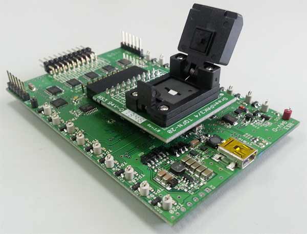
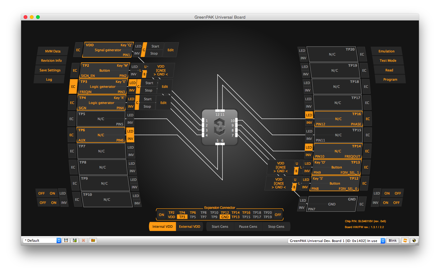
The Greenpak3 development kit comes with a nice little test and programming board and a bunch of samples of the various chips in the range. The development board supports what they call ‘emulation’, but what it’s actually doing is writing your design to the chip in temporary memory so you can test it out. You can do this as many times as you want, but once you program it for real, that’s it: your chip will only ever function like that, no backsies.

On the dev board, there’s testpoints for each of the pins on the chip, and the IDE has a very nice interface to send digital and analog waveforms to the chip, as well as enabling the onboard LEDs, and configuring keyboard shortcuts to turn signals on and off. You can hook your scope up to the test points, or input signals on the expansion connector.

Naturally, I whipped out the devkit and set to work trying to see if I could implement my required logic on one of their cheap-as-chips chips. Their IDE uses a drag-and-drop style of programming, drawing wires between inputs and outputs in a manner that will be familiar to anyone who’s used an EDA tool before. Individual components are configured by clicking them, where settings can be set, and truth tables entered.
I wanted my new chip to do three things:
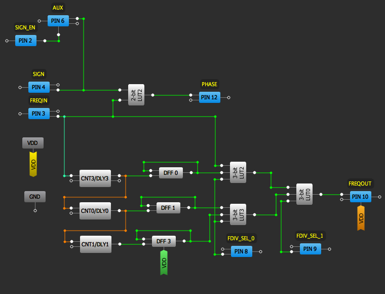
After an hour or so’s work, I had this to show for myself:

In the top left the square wave signals from the input comparator and the DDS chip come in on pins 3 and 4, respectively. The component marked “2-bit LUT2” implements the original functionality of the XOR IC, outputting the resulting signal on Pin 12. That’s goal 1 sorted!
Pin 2 acts as an output enable for the DDS’s square wave output on pin 6, which is connected to the AUX connector. There’s goal 2.
The rest of the circuit is concerned with implementing the frequency divider. In brief, the signal coming in on pin 3 is fed into a series of chained counters (CNT0/DLY0, 1, and 3), each one dividing it down further. A flipflop on the output of each takes the short pulse each counter outputs when it overflows and turns it into a proper 50% duty cycle square wave. And the three components marked LUT0, LUT2, and LUT3 act as a 4:1 multiplexer, allowing two external pins to control which of the divided signals gets output to the microcontroller. Presto, goal 3: selectable frequency division by 1, 16, 256 or 4096.
Another hour’s work with the devkit, emulator, and my scope, and I was able to verify that everything behaved as expected. And half an hour in diptrace proved that removing the XOR and adding this new chip was quite straightforward. I still had time to rush the design revision off to Macrofab before they sent the release candidate 1 boards off for production.
This also feels like significantly less design risk and cost than integrating two new chips to perform this function; if that were the only option, the Tsunami would have remained as it was. As it is, I’m waiting for the first releease candidate boards so I can run a full set of tests in-situ, but I’m very optimistic. For the cost of 8 cents per Tsunami and a few hours of my time, I was able to add some truly useful new features.
It’s hard to see why these little chips aren’t more popular and well known, especially with hobbyists, than they are now. They’re really cheap, the devkit is affordable at only $60, and Silego will produce a run of chips preprogrammed with your design on tape-and-reel at quantities starting at 1, for a very nominal price; the $0.50 price I keep quoting includes programming at quantities from 250 units and up. The IDE is available for Windows, Mac, and Linux.
Their datasheets even fully document the bitstream the chips use for programming; this chip is just dying for someone to write a VHDL or Verilog compiler for it.
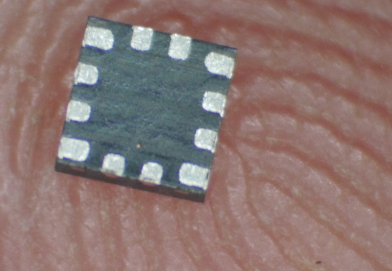
There’s just one thing: these little chips really are just that: little. The standard package is an 0.4mm pitch QFN. The part I’m using has 12 pads, which means it’s only 2mm on a side. For a sense of scale, here’s me holding one.

Yes, that’s the pad of my thumb. These things really are tiny, and that really can be a bit of an impediment. Anyone with a soldering iron, some flux, and a bit of magnification can solder these - though having hot air certainly makes life simpler - but prototyping on a breadboard is going to be tough, and they certainly require a bit of patience to get right by hand on a PCB, unless you’ve got stencils and solderpaste.
The obvious solution to this is breakout boards; you’ll still need to solder them on, but from there you can plug them into a breadboard and use them like regular DIP chips. Or, to take it a step further, prepopulated breakouts, and an adapter for their excellent devkit to allow programming them in that form factor. Any takers?
Full disclosure: I don’t have any association with Silego or their parts other than being a happy customer. I just think their stuff is neat, and wanted to tell people about it.